X Eagle Top Gear: High-Speed PCB Design Meets Automotive Innovation - Calculate trace length from time delay value for high speed pcb design ...
If you are looking for Calculate Trace Length From Time Delay Value For High Speed PCB Design you've visit to the right web. We have 35 Pics about Calculate Trace Length From Time Delay Value For High Speed PCB Design like Webinar-Mastering Design for Excellence(DFx) in High-Speed PCB Design, Top Challenges in High-Speed PCB Design: How to Overcome and also High-Speed PCB Design Routing Strategy. Read more:
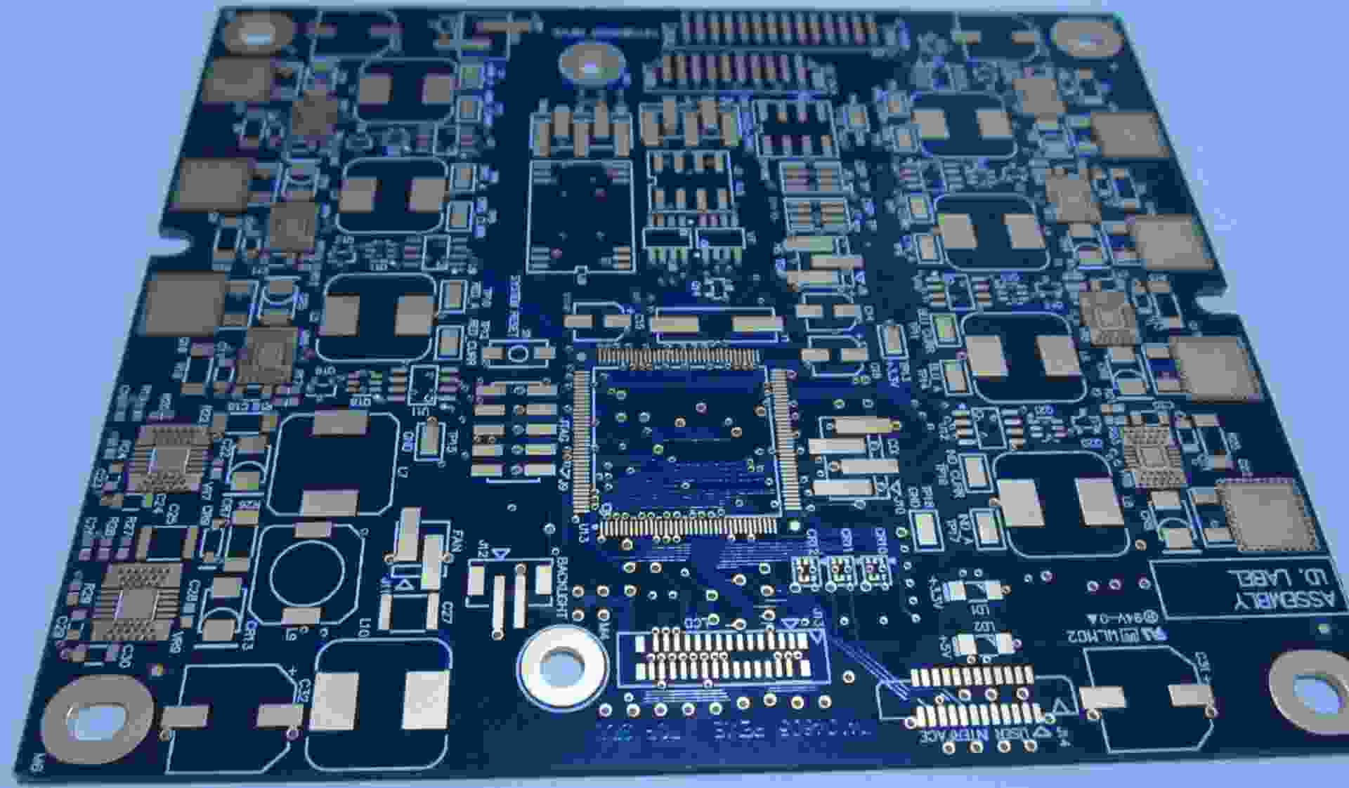
Calculate Trace Length From Time Delay Value For High Speed PCB Design
 pcb-copy.com
Calculate Trace Length From Time Delay Value For High Speed PCB Design ...
High-Speed PCB Design Fundamentals: Key Insights For Success
 jamindopcba.com
High-Speed PCB Design Fundamentals: Key Insights for Success
Understanding High-Frequency And High-Speed PCB Design | Viasion
 www.viasion.com
Understanding High-Frequency and High-Speed PCB Design | Viasion
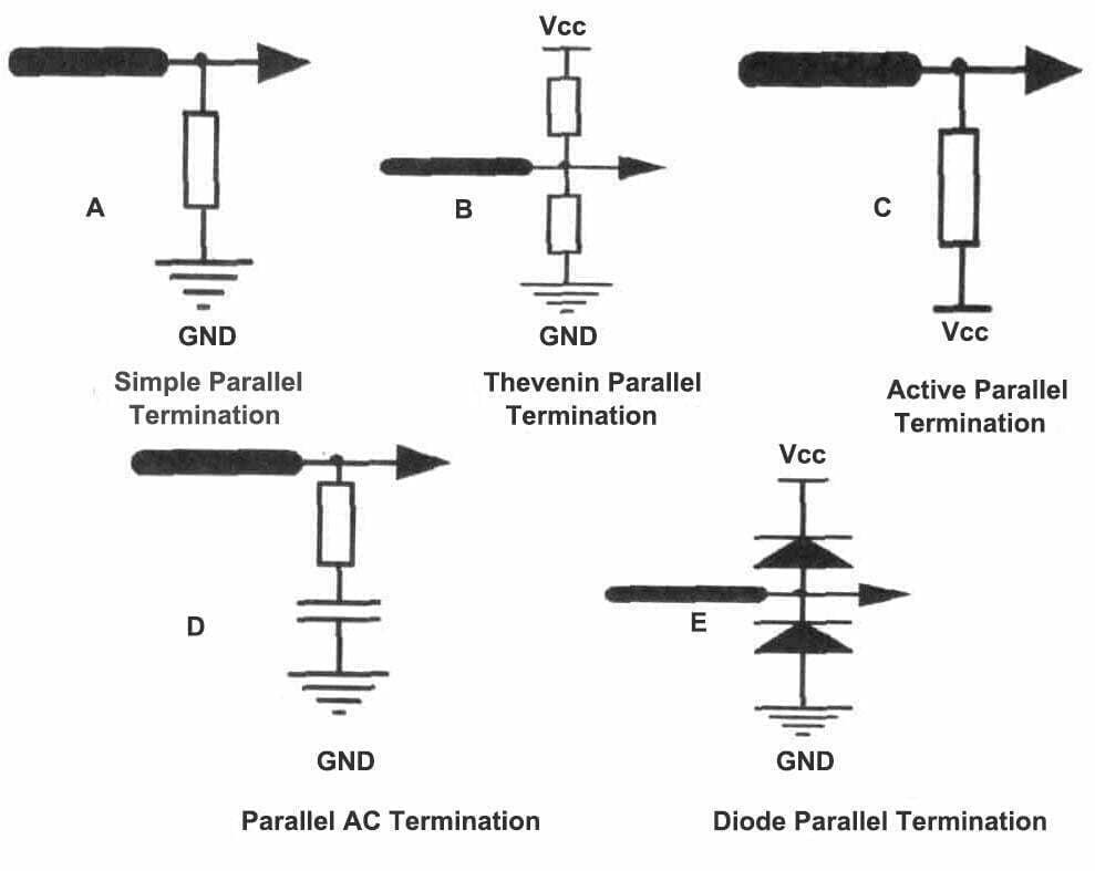
High Speed Pcb – Pcb Haute Vitesse Pdf – ZRPIV
 shape.hotpeachpages.org
High Speed Pcb – Pcb Haute Vitesse Pdf – ZRPIV
High Speed PCB Design Fundamentals
 www.pcbtok.com
High Speed PCB Design Fundamentals
Signal Integrity Analysis In High Speed PCB Design | Reversepcb
 reversepcb.com
Signal Integrity Analysis In High Speed PCB Design | Reversepcb
High Speed Pcb – Pcb Haute Vitesse Pdf – ZRPIV
 shape.hotpeachpages.org
High Speed Pcb – Pcb Haute Vitesse Pdf – ZRPIV
High-Speed PCB Design Guide For Production
 hilelectronic.com
High-Speed PCB Design Guide for Production
High-speed Pcb Design Guide - Andwin Circuits
 www.andwinpcb.com
High-speed pcb design guide - Andwin Circuits
Understanding High-Frequency And High-Speed PCB Design - Viasion PCB
 www.viasion.com
Understanding High-Frequency and High-Speed PCB Design - Viasion PCB
High-Speed PCB Design Guides | Research, PCB Design & Layout, Embedded
 www.nwengineeringllc.com
High-Speed PCB Design Guides | Research, PCB Design & Layout, Embedded ...
High Speed PCB Design: Routing, Impedance & Layout Techniques
 hackatronic.com
High Speed PCB Design: Routing, Impedance & Layout Techniques
Mastering High-Speed PCB Design: Key Techniques & Tips - GlobalWellPCBA
 www.globalwellpcba.com
Mastering High-Speed PCB Design: Key Techniques & Tips - GlobalWellPCBA
Webinar-Mastering Design For Excellence(DFx) In High-Speed PCB Design
Webinar-Mastering Design for Excellence(DFx) in High-Speed PCB Design ...
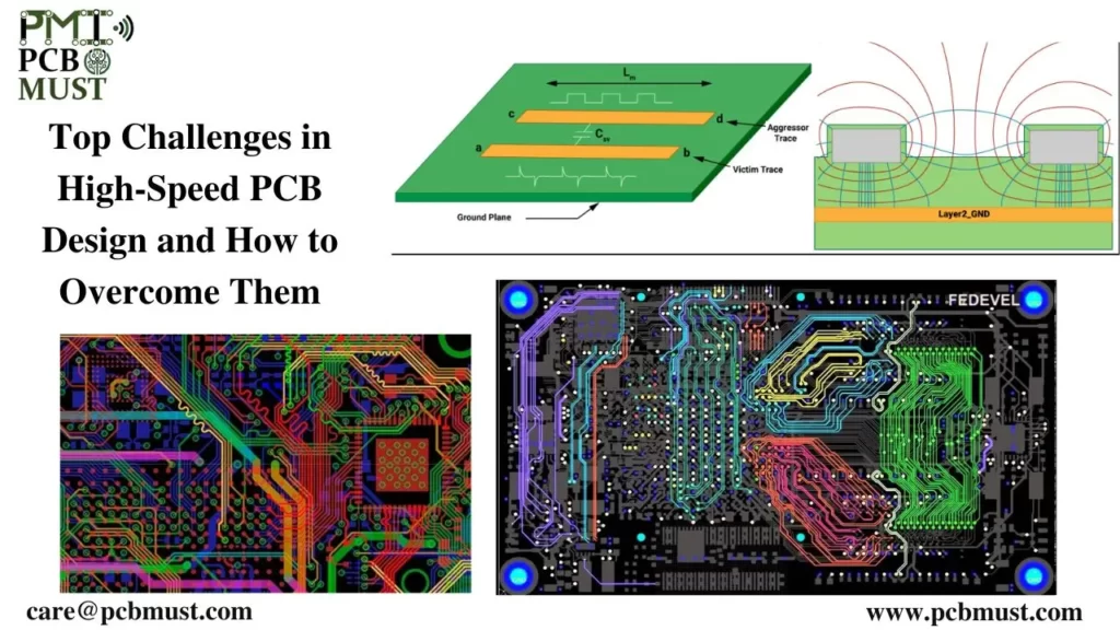
Top Challenges In High-Speed PCB Design: How To Overcome
 pcbmust.com
Top Challenges in High-Speed PCB Design: How to Overcome
Understanding High-Frequency And High-Speed PCB Design | Viasion
 www.viasion.com
Understanding High-Frequency and High-Speed PCB Design | Viasion
High Speed Pcb Design And Layout, Expert PCB Design Service [ With Step
 www.venture-mfg.com
High Speed Pcb Design and Layout, Expert PCB Design Service [ With Step ...
The High-Speed PCB Stackup Design Challenge | High-Speed Design
 resources.altium.com
The High-Speed PCB Stackup Design Challenge | High-Speed Design
High-speed PCB Design: An Essential Guide For Professionals - MainPCBA
 www.mainpcba.com
High-speed PCB design: an essential guide for professionals - MainPCBA
High-Speed PCB Design: 7 Key Rules | Twisted Traces
 www.twistedtraces.com
High-Speed PCB Design: 7 Key Rules | Twisted Traces
High-Speed PCB Design: Best Practices For Routing And Placement
 southelectronicpcb.com
High-Speed PCB Design: Best Practices for Routing and Placement
The Ultimate Guide To High-Speed PCB Design- Jarnistech
 www.jarnistech.com
The Ultimate Guide to High-Speed PCB Design- Jarnistech
High-Speed PCB Design And The Impact Of EMI Shielding
 mars-pcb.com
High-Speed PCB Design and the Impact of EMI Shielding
Different Types Of Vias In High Speed PCB Design
 pcbmust.com
Different Types of Vias in High Speed PCB Design
7 Essential Principles For High-Speed PCB Design- Jarnistech
 www.jarnistech.com
7 Essential Principles for High-Speed PCB Design- Jarnistech
What Is High-Speed PCB Design And Guidelines? | Viasion
 www.viasion.com
What is High-Speed PCB Design and Guidelines? | Viasion
What Is High Speed PCB Design - Keep Best PCBA
 www.keepbestpcba.com
What Is High Speed PCB Design - Keep Best PCBA
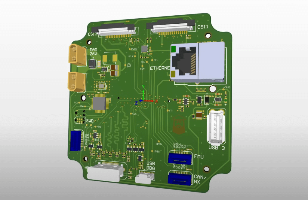
High-Speed PCB Layout Design Guide -101 - Embedded Hardware Design
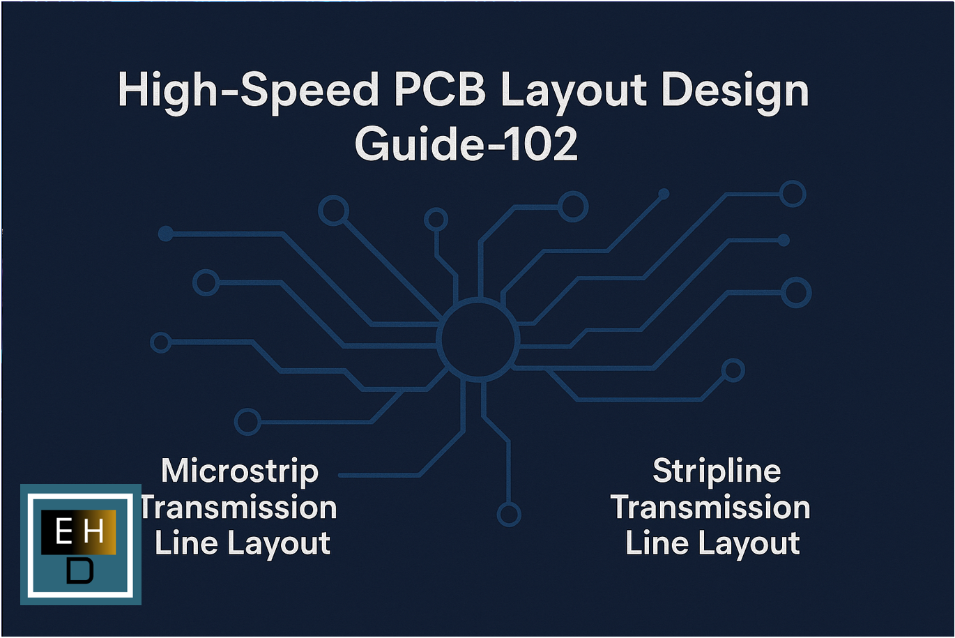 embeddedhardwaredesign.com
High-Speed PCB Layout Design Guide -101 - Embedded Hardware Design
High Speed PCB Design Routing And Layer Stackup Techniques
 www.viasion.com
High Speed PCB Design Routing and Layer Stackup Techniques
High-Speed PCB Design Tips And Guidelines | Phil's Lab | Altium Designer
 resources.altium.com
High-Speed PCB Design Tips and Guidelines | Phil's Lab | Altium Designer
Comprehensive Guide To High-Speed PCB Manufacturing And Design- Jarnistech
 jarnistech.com
Comprehensive Guide to High-Speed PCB Manufacturing and Design- Jarnistech
Comprehensive Guide To High-Speed PCB Design
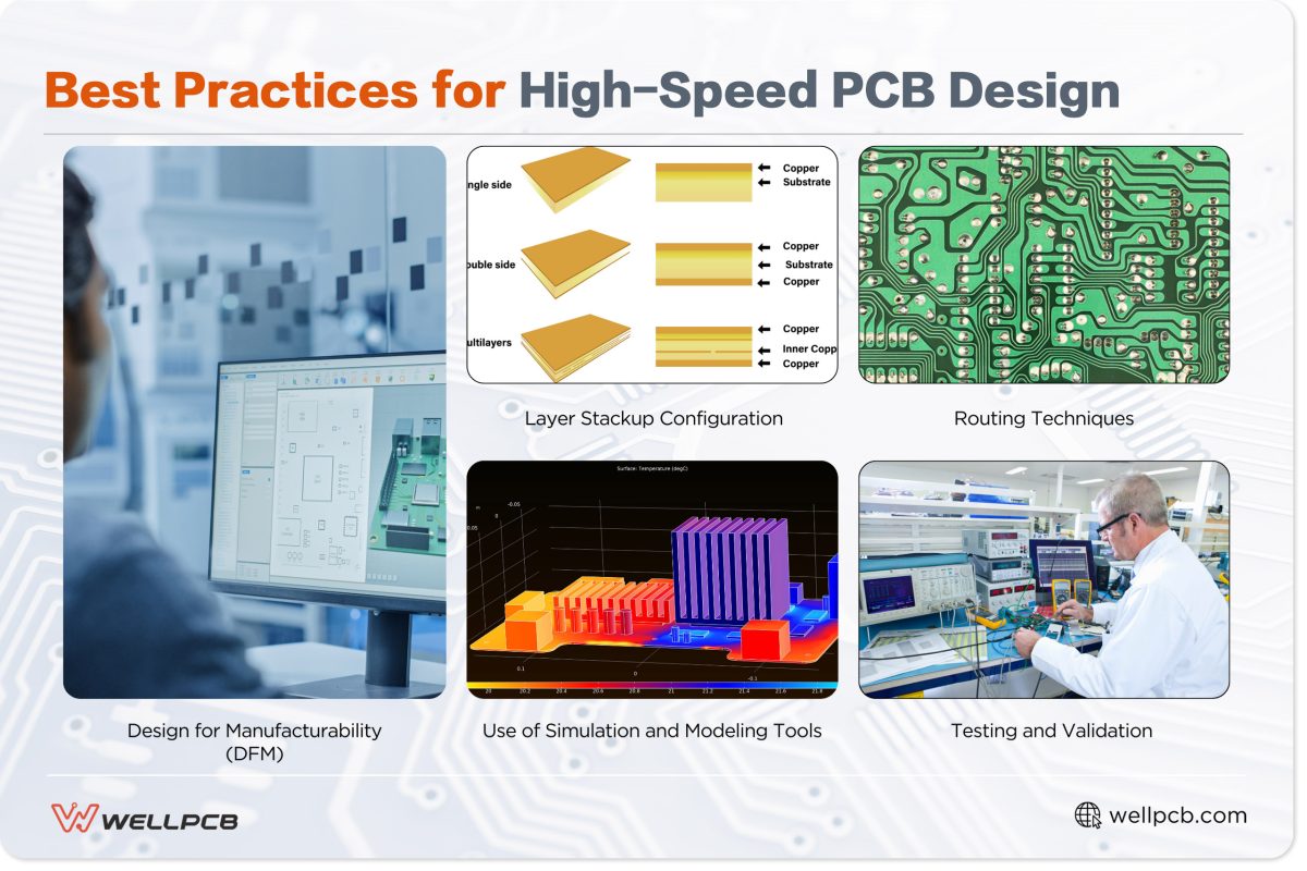 www.wellpcb.com
Comprehensive Guide to High-Speed PCB Design
Understanding High-Frequency And High-Speed PCB Design | Viasion
 www.viasion.com
Understanding High-Frequency and High-Speed PCB Design | Viasion
PCB Factory: High-speed PCB Design Sharing Based On Cadence - Kingford
 www.kingfordpcb.com
PCB factory: high-speed PCB design sharing based on Cadence - Kingford
High-Speed PCB Design Routing Strategy
 www.linkedin.com
High-Speed PCB Design Routing Strategy
The high-speed pcb stackup design challenge. Comprehensive guide to high-speed pcb design. top challenges in high-speed pcb design: how to overcome